
News
AI Solvent Recipe Doubles QLED Efficiency, Lifts Lifetime 40-Fold
An AI-designed solvent blend doubled QLED efficiency and extended lifetime 40-fold, joining the same inverse design wave already reshaping battery research.

An AI-designed solvent recipe made a lab-built quantum dot display run nearly twice as bright and last more than 40 times longer, South Korean researchers reported July 15. The team, based at Seoul National University and Sungkyunkwan University, used machine learning to solve a problem that had mostly been attacked by guesswork: which liquid to dissolve quantum dots in before coating them onto a screen.
The same inverse design trick, telling a model what outcome you want and asking it to work backward to a recipe, has already turned up new battery materials and mapped millions of untested crystal structures elsewhere in the lab. Now it has reached the chemistry behind the television screen.
Why the Solvent Decides a Quantum Dot’s Fate
Quantum dot LEDs, or QLEDs, use nanometer-scale semiconductor particles as their light-emitting layer. Their appeal is that they can be built through a liquid coating process rather than the vacuum deposition that OLED panels require, which is what makes them cheap to scale to large screens.
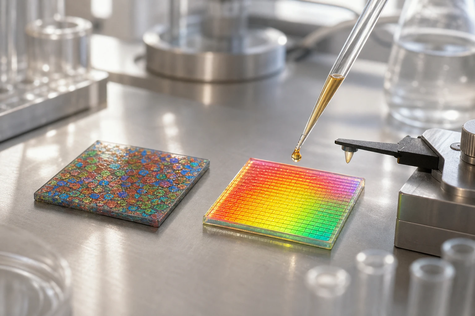
That same liquid process is where the trouble starts. To achieve high-performance QLEDs, quantum-dot particles must be arranged uniformly and densely within the thin film, much like bricks. The challenge is that the choice of solvent used to form the film in this solution process significantly affects brightness and lifespan.
Predicting which solvent produces which outcome has been mostly guesswork. Engineers would mix a batch, coat a film, test it, and try again, a cycle that eats time and money without any guarantee of a better result.
Teaching an AI to Read a Thin Film
To break that cycle, the joint team led by Professor Jeonghun Kwak of Seoul National University’s Department of Electrical and Computer Engineering and Professor Jaehoon Lim of Sungkyunkwan University’s Department of Energy Science built a machine learning model that connects a solvent’s physical fingerprint to how the resulting quantum dot film actually looks under a microscope.
They started by coating films with five representative solvents and scanning each one with atomic force microscopy, a technique that uses a fine probe to map a surface’s height and roughness. The model then learned the relationship between a solvent’s measurable traits and how tightly its quantum dots packed together. Among the properties it weighed:
- Vapor pressure, which affects how fast the solvent evaporates during coating
- Viscosity, which shapes how the liquid spreads across the substrate
- Density, which influences how quantum dots settle as the film dries
- Dielectric constant, which affects how the dots interact with each other in solution
Once trained, the model could run the process in reverse. Instead of predicting how a given solvent would behave, it could specify the ideal solvent profile for the most uniform packing and let researchers chase that target.
The Blend Nobody Would Have Tried
Here is where the project could have stalled. No single solvent possessed all of the optimal properties suggested by the AI, so the research team combined multiple solvents to realize the conditions the AI had proposed. It was a complex combination that would have been difficult to discover through repeated experimentation alone.
They built that blend into an actual QLED, not a simulation. Applied to a real fabrication process, it produced roughly double the efficiency and more than a 40-fold increase in operating lifetime compared with devices made using a single conventional solvent.
This research demonstrates that AI can be used to design display materials and processes on a data-driven basis.
Kwak, who led the study, said the payoff extends beyond one display technology. He expects it can also be applied to the development of various next-generation electronic devices, including OLEDs and solar cells. The work, led by researcher Beomsoo Chun, was published in Reports on Progress in Physics, a journal from the United Kingdom’s Institute of Physics, and was supported by Korea’s Ministry of Science and ICT and the National Research Foundation of Korea through the Future Display Leading Technology Program and the Nano and Material Technology Development Program.
DeepMind and Microsoft Already Ran This Playbook
Asking a model to work backward from a target property to a workable recipe is not new. It is the same idea behind two of the biggest materials-science stories of the past three years, just aimed at a different problem.
In 2023, researchers at Google DeepMind and Lawrence Berkeley National Laboratory announced a system called GNoME that discovered over 2 million new materials that could be used to develop technologies like batteries, solar panels, and computer chips. Over 17 days, the system identified 2.2 million potentially stable crystal structures, more than 700 of which have already been experimentally validated.
Microsoft took a related approach in January 2025 with MatterGen. Rather than screening millions of existing compounds, the traditional approach that can take years, MatterGen directly generates novel materials based on desired characteristics, similar to how AI image generators create pictures from text descriptions. In one demonstration, Microsoft researchers said the tool took a screening process that would have taken many years of compute by conventional methods and reduced it to just 80 hours of computation, producing a candidate that became a battery built with 70 percent less lithium than a standard cell.
Three teams, three material classes, one shared method: train a model on the link between structure and performance, then ask it to work backward to a recipe.
| AI Materials Platform | Built By | Published | Headline Result |
|---|---|---|---|
| Inverse solvent design | Seoul National University and Sungkyunkwan University | Reports on Progress in Physics, July 2026 | Roughly 2x QLED efficiency, more than 40x operational lifetime |
| GNoME | Google DeepMind and Lawrence Berkeley National Laboratory | Nature, November 2023 | 2.2 million new crystal structures predicted, over 700 validated in the lab |
| MatterGen | Microsoft Research | Nature, January 2025 | Generates candidates directly instead of screening; prototype battery cut lithium use 70% |
Samsung, LG and a Billion-Dollar Race for a Better Pixel
None of this happens in a vacuum. Quantum dot displays already sit inside a growing consumer electronics category, and efficiency and lifetime are the two numbers that decide how expensive a panel is to build and how long it survives in a living room.
- $1.9 billion: the projected 2026 value of the global quantum dot display market, on its way to $5.9 billion by 2035 at a 13.3% annual growth rate.
- 73%: the combined 2025 market share held by the top five quantum dot suppliers, led by Nanosys at 21.3%, ahead of Samsung Display, Samsung Electronics, LG Display and Sony.
- 2.5 million: QD-OLED monitor panels Samsung shipped in 2025 alone, part of cumulative shipments topping 5 million units by March 2026.
A method that doubles efficiency and multiplies lifetime by 40 times matters to that list of companies for a plain reason: fewer failed panels, less wasted material, and a brighter screen for the same power draw. None of the manufacturers named above have said publicly whether they plan to test the Seoul team’s approach.
How Close Is This to an Actual TV Screen?
Not close yet. The result is a peer-reviewed laboratory demonstration built and measured by an academic team, not a manufacturing process running on a factory line, and the researchers have not published a timeline for scaling the multi-solvent blend beyond their own devices.
What we know:
- The efficiency and lifetime gains were measured in real fabricated QLEDs, not computer simulations alone.
- The study passed peer review and was published in a recognized international physics journal on July 15.
- Two Korean government programs funded the work, signaling continued institutional backing for the approach.
What’s unconfirmed:
- Whether the technique works as well on the cadmium-free, indium phosphide quantum dots that regulation is pushing manufacturers toward.
- Whether the multi-solvent blend can be produced at the volume and cost a TV factory needs.
- Whether any display maker has begun testing the method outside the university labs that developed it.
Kwak’s own framing points to where this goes next. Solar cells and OLED lighting run on the same solution-processing logic as QLEDs, meaning the same inverse design model could, in theory, be retrained on a different material stack without starting from zero.
Frequently Asked Questions
What exactly is a quantum dot?
Quantum dots are semiconductor nanocrystals roughly 1.5 to 5 nanometers in diameter that produce pure red, green or blue light through quantum confinement effects. Their exact size, not their chemical formula alone, is what determines the color they emit, which is why uniform packing during manufacturing matters so much.
Why are display makers moving away from cadmium-based quantum dots?
Cadmium is a restricted heavy metal under European Union rules, and EU RoHS cadmium-restriction mandates are pushing the cadmium-free quantum dot share toward 75% of the materials market by 2027. That regulatory shift is a separate pressure on manufacturers, running alongside any efficiency gains an AI-designed process might eventually deliver.
Is the AI-designed QLED already available to buy?
No. This is a university research result, not a commercial product. There is no announced consumer device, licensing deal or production timeline tied to the solvent platform described in the study.
Was the AI’s solvent recipe tested in a real device or just modeled on a computer?
It was built into a working device. The researchers fabricated actual QLEDs using the AI-recommended solvent blend and measured efficiency and operational lifetime directly, rather than relying on simulated predictions alone.
How does this compare to AI projects like GNoME and MatterGen?
GNoME and MatterGen mostly generate candidate materials that still need to be synthesized and verified in a lab before anyone knows if they work. The Seoul and Sungkyunkwan team already closed that loop, building its AI’s recommendation into hardware and measuring the result, which is a further step down the path from prediction to a working part.


Walmart’s $50 Million Opioid Settlement Closes Case Without Admission

California Sues Over $120 Million Morro Bay Wind Lease Buyout

Gilead Bixlenvo FDA Nod Opens Single Pill Path for Complex HIV Cases

Meta’s $18B Kids Deal Forever Shields Data Used to Spot Under-13s

Lettuce Outbreak Drove Record Cyclospora Spike Across 20 States

Amazon Shaves $20 Off M6 Mac Mini Before It Even Ships

SpaceX Louisiana Port Tests Debt Markets on Orbital AI Scale

Microsoft High Lifts Indexes as Small Caps Crack Support

Apple Replays 2015 Saturday Midnight Preorder for iPhone 18 Pro

Updated COVID Shots Clear FDA but Access Friction Hits High-Risk Groups

Take-Two CEO Pushes Netflix Subs for GTA 6 Extended Look

Wildlands Free Update Hands Players the Tools They Already Invented

Destiny 2 Fans Unlock Vaulted Maps After Live Service Ends

Quake Gets 19 Free Maps From MachineGames Quake Club

Quordle Monday Delivers Gavel Crush Speed Ethos Cleanly

Stripe Bid Shows PayPal Moat Cracked After Years of Slide

Tyson’s Five-Year Utah Plant Falls to Cattle Shortage Reckoning

Silver Lake Workday Talks Signal Private Floor for Software

Kennedy Lewis Takes Majority Control of The Greenbrier in $500M Deal

Best Buy Marks 60 Years With Sale That Echoes Its Audio Shop Roots
-

 TECHNOLOGY3 years ago
How to Adjust a Bulova Watch Band – An Easy Guide
-

 News3 years ago
Fred Pentland: Athletic Bilbao’s English mentor who changed the essence of Spanish football
-

 FINANCE3 years ago
Tax Planning for Every Season: Guide to Maximizing Your Tax Benefits
-

 Education3 years ago
African Ministers New Education Plan
-
 BUSINESS3 years ago
What is Entrepreneurial Operating System? A Comprehensive Guide to EOS
-

 Education3 years ago
Innovate Your Learning Journey with Technology and Enhance Education
-

 News3 years ago
Russians formally out of World Athletics Championships
-

 BUSINESS3 years ago
Top 9 Most Expensive American Cities to Rent an Apartment